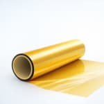
Asahi Kasei announced the development of a new photosensitive polyimide PSPI film intended for advanced panel-level semiconductor packaging. The panel-level packaging segment is gaining importance in the semiconductor industry as manufacturers seek higher efficiency and improved yield in processes that meet the requirements of next-generation semiconductor packaging. In response to these market changes, the company combined the properties of its photosensitive polyimide PSPI resin and dry film photoresist DFR in a new film material. According to the company, the solution is currently under customer evaluation, and commercial availability is expected in the near future.
The new PSPI film was developed based on Asahi Kasei's expertise in the production of PIMEL liquid PSPI, used in buffer coatings and passivation layers, and SUNFORT dry film photoresist for temporary lithographic circuit patterning on substrates and wafers. According to the company, the material is intended to improve productivity in semiconductor packaging manufacturing by enabling easy and uniform application in a lamination process on large square panels. In addition, the film was designed to support an increased number of insulating layers. It is expected to be used in redistribution layers for semiconductor packaging and in insulating layers for package substrates.
Combining PSPI and dry film photoresist functions
Asahi Kasei indicates that combining the new PSPI film with the Sunfort TA series, capable of forming circuits with a width of 1.0 μm, makes it possible to form both fine circuit patterns and insulating resin layers by film lamination. The company is also developing solutions that combine the PSPI film with the Sunfort CX series. This approach is intended to enable the formation of high-aspect-ratio copper pillars required in three-dimensional semiconductor packaging.
Nobuko Uetake, Senior Executive Officer at Asahi Kasei responsible for the Electronic Materials MBU, said: "As the performance of AI semiconductors improves, advanced semiconductor packaging requires mounting technologies that cover larger areas and offer higher precision. Through our new PSPI film product, we aim to contribute to our customers' improved yield and productivity, while supporting the further evolution of advanced semiconductor packaging."
Rising requirements for electronic materials
Electronics has been designated as one of the priority business areas in Asahi Kasei's medium-term management plan, Trailblaze Together. Electronic materials such as PIMEL PSPI and Sunfort dry film photoresist are used in advanced semiconductor packaging applications. Demand for such materials continues to rise as chips are packaged at higher density and interposers become larger, driven by the requirements of AI data centers.
The company also emphasizes that wiring patterns are becoming finer and the number of layers is increasing as packaging moves from wafer-level to panel-level and develops toward more three-dimensional structures. This in turn increases the performance requirements for materials used in semiconductor packaging.